The Calculation of Output DC Offset for ACOT® Control Buck Converter with Feed-forward Compensator
Abstract
With the increasing focus on reliability and size consideration of converter design, the ceramic capacitors become more and more popular in NB applications. Hence, the Advanced Constant On-Time (ACOT®) control topology has been developed to provide stable operation for ceramic output capacitors without complicated external compensating networks. Generally, the stability is always the top concern for the designer. In many cases, in order to enlarge the noise margin and transient speed of feedback loop, the traditional voltage divider is replaced with feed-forward compensator. However, an additional dc offset will be generated on the output voltage which comes from output voltage ripple and feed-forward compensator due to valley control of output. Especially, the different pole and zero placement of feed-forward compensator will make the distortion and phase movement on feedback signal. This may influence the regulating accuracy and maximum value of output voltage. In this application note, detailed analysis and derivation about dc offset will be presented and discussed.
1. The Introduction to ACOT® Control and
Feed-forward Compensator
Before starting to calculate the quantity of dc offset, it deserves to reserve some time to introduce and understand the mechanism of ACOT® control topology. Moreover, the feed-forward compensator characteristics and effects on feedback signal will be discussed in the later.
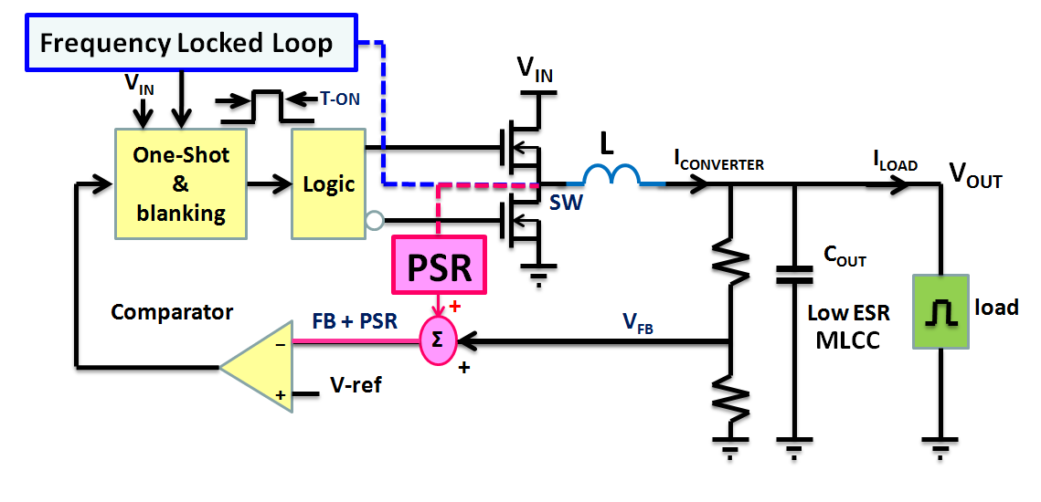
Figure 1. A Buck Converter with ACOT® Control Method
Figure 1 illustrates a standard ACOT® control Buck converter. Unlike traditional constant on-time control method which requires large output capacitor ESR to generate the current ramp signal on feedback voltage for stable operation, an internal pulse-shaping-regulator (PSR) is applied to generate the equivalent inductor current ramp voltage. By comparing the composed signal of PSR and feedback voltage with reference voltage, an on-time one-shot circuit will be triggered as the composed signal below reference voltage. Besides, for constant frequency operation in CCM, a frequency locked loop is applied to adjust on-time period dynamically. Contrarily, fixed on-time enables the reduction of switching frequency during the light load operation, and the smaller switching loss will improve the light load efficiency in DEM. Moreover, faster transient response and no need for additional slope compensator make ACOT® control method become more popular.
The operating behavior of ACOT® control loop in CCM and DEM are demonstrating in Figure 2 and Figure 3 separately. In CCM operation, the PSR circuit generates the ramp signal by subtracting VB with VA to acquire the signal of VC, where VA and VB are the internal signals via detecting the switching node signal. The composed signal of VC and reference voltage will then be used to compare with feedback voltage in closed loop control. Meanwhile, the dc offset of ramp ripple can be properly eliminated by an internal sample and hold circuit of PSR. However, due to the valley control of output voltage, the output ac ripple will create another dc offset on output voltage. This may influence the accuracy of control and restrict the design margin of output voltage. In the other hand, while in DEM operation, the three different conditions of switch conduction are considered and keep ramp voltage flat as inductor current reduce to zero. This is indispensable for stable loop control in DEM operation. Likewise, the output ac ripple will contribute additional dc offset on output voltage.
|
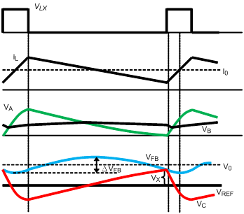
Figure 2. ACOT® Control in CCM
|
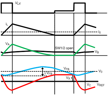
Figure 3. ACOT® Control in DEM
|
As mentioned in previously, the feed-forward compensator is usually added to improve the noise margin and transient performance. For a typical feed-forward compensator as Figure 4, one pole and zero are generated to perform as a high-pass filter which means the gain magnitude will change according to different frequency locations of output signal. Also there is an additional phase lead on feedback that affects the dc offset on output voltage. The transfer function from VOUT to VFB can be derived as equation (1), and an example is given to make more easily realize in Figure 5. The dc gain of A(s) is equal to 1 / (1 + R1 / R2), and staring to increase at the frequency of zero and then decrease at the frequency of pole. The pair of pole and zero provides a phase leading on feedback signal, and the maximum phase leading is 51.8˚ for this example. In the example bode plot, the gain and phase are -13.4dB and 46.7˚ respectively at switching frequency.
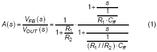
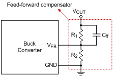
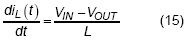
Figure 4. Feed-forward compensator in feedback loop
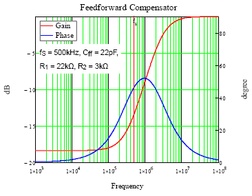
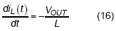
Figure 5. Bode Plot of A(s)
2. The Calculation of Output DC Offset in DEM
For a Buck converter with constant on-time control and operates in light load, the inductor current may reaches to zero when off-time is large enough to discharge the inductor current. If the current reaches to zero, the low-side switch will then turn off and high-side switch remains off. At this moment, there is no current flowing through the inductor. However, the high-side switch will remain off until output voltage decreases lower than the reference voltage. During the both off state, the residual charge in the output capacitors is discharged by load current. Therefore, the switching frequency will vary with the load current in DEM. The relation of switching frequency and load current can be derived as :
, where the Fs is the switching frequency of converter, Vin is the input voltage of converter, Vout is the output voltage of converter, Io is the load current and Ton is the on-time period of high-side switch. It can be observed that switching frequency is proportional to the output load.
Due to the piecewise linear characteristic of inductor current in DEM, the output voltage ripple consists of a lot of components with different frequencies. It makes it infeasible to look output voltage ripple as a single frequency signal. Fortunately, all of the periodical signal can be decomposed to a composition of variety of sine and cosine functions. In the light of linearity and time shift properties of Fourier transform, it makes a sense that multiplying the gain and phase at specific frequency for each decomposed function when considering about the feed-forward compensator. Therefore, the output voltage ripple can be expanded as a Fourier series. Before define the steady state equation of output voltage ripple, the inductor current should be realized. The following equations state the variation rate of the inductor current at different switching status for a single switching cycle.
For the period during high-side switch is turned on,  :
:

For the period during low-side switch is turned on,  :
:
For the period during all switches are turned off,  :
:
, where Ts(Io) is the switching period at Io and Toff is the turning on duration of low-side switch.
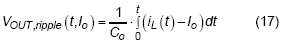
Then the output voltage ripple can be derived from above equations, as stated in below :
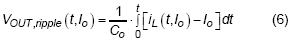
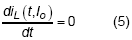
, where Co is the output capacitor and it should be noticed that both of iL and Vout,ripple are the functions of time and Io, the switching period will change with load current. It should be noticed that only AC ripple is considered in equation (6), the DC value is not important here.
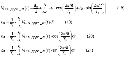
Next step, the Fourier series is adopted for representing the function of output voltage ripple. Following are the equations of output voltage ripple in Fourier series with N order expression :
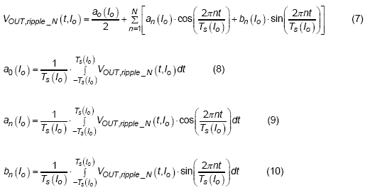
The function of output voltage ripple can be represented as a series of coefficients time sine and cosine functions of different frequencies. The coefficients can be derived by multiply to sine or cosine functions of different frequencies and apply the integral to acquire the average value. Where the a0 (Io) is the coefficient of dc component when output load current is equal to Io, the an (Io) are the coefficients of cosine functions of different frequencies for different load current and the bn (Io) are the coefficients of sine functions of different frequencies for different load current.
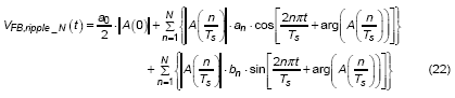
As the Fourier expression of output voltage ripple is defined, the next step is to use these functions as the input for feed-forward compensator, A(s). In order to process the multiplication of two functions in time-domain more efficiently, then apply the convolution property of Fourier transform. The convolution property makes it possible for two functions in time domain to multiply each other in frequency domain. Therefore, the description of feedback signal in time domain can be derived as following :
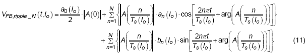
, where the A(0) is the dc gain of feed-forward compensator, | A (n / Ts (Io) ) | is the gain at specific frequency of (n / Ts (Io) ) and arg ( A (n / Ts (Io) ) ) is the phase shift at the frequency of (n / Ts (Io) ).
Because of the feed-forward compensator and output voltage ripple, an additional dc offset will be generated. In order to describe the value of dc offset, it is a good way to discuss with a picture. As shown in Figure 6, there are three signals used to describe the origin of this offset , for the first one, the red waveform with solid line, is named “Original VFB without phase shift”, it displays the feedback signal only with magnitude change but no phase shift. In this case, there is only partial dc offset produced by the ripple voltage of VFB. For the second one, the red waveform with dotted line named “Original VFB with phase shift”, the phase shift is also considered, and it can be noticed that the VFB is lower than the Vc when the gate signal of high-side MOSFET (UG) is triggered. Due to the valley control mechanism, the final VFB in loop control will then be the blue waveform with solid line, is named “VFB with Feed-forward in loop”. It can be observed that an additional dc offset, Dy1, has been generated. The formula of Dy1 and the average of feedback voltage ripple can be derived as :
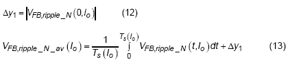
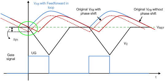
Figure 6. The relation of feedback signal and internal ramp signal in DEM
3. The Calculation of Output DC Offset in CCM
When converter operates in CCM, the frequency is well regulated as a constant. Unlike in DEM as discussed before, inductor current is always above zero. At stable operation, the duty cycle can be decided by the input and output voltage.
For the period during high-side switch is turned on,  :
:
For the period during low-side switch is turned on,  :
:
, where Ts(Io) is the switching period at Io and Toff is the turning on duration of low-side switch.
Then the output voltage ripple can be derived from above equations, as stated in below :
, where Co is the output capacitor, the dc value of Io will not change the switching frequency in CCM, therefore, only ac ripple will be considered in following derivation.
Same as the analysis in DEM condition, the Fourier series of CCM output voltage ripple is also derived as equation (18)~(21).
Apply the convolution property to process the multiplication of two functions in frequency domain then transfer back to time-domain as equation (22).
As depicted in Figure 7, three waveforms are used to describe the origin of additional dc offset which comes from phase shift. Similar story as describe in DEM section, an additional dc offset value of Dy2 has been generated and make final output voltage to locate under or above the preset value.
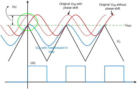
Figure 7. The relation of feedback signal and internal ramp signal in CCM
4. Verification via Simulation and Experiment
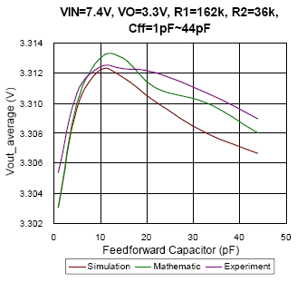
The detailed derivation and description of the origin of output dc offset has been given in the previous sections. The major purpose here is to verify the accuracy of the derived formula. A practical example of RT6220 ACOT® control converter is selected to verify the calculation result. The detailed setup for simulation and experiment are listed in the Table 1. And the results are depicted in Figure 8 and Figure 9. The comparison results between them will be discussed later.
Table 1. Simulation and Experiment Parameters Setup
|
Operating Condition
|
VIN
|
Vref
|
Voltage Divider
|
Cff
|
|
DEM (Io = 0.15~1.6A)
|
7.4V/12V/19V
|
0.6V
|
R1 = 162k, R2 = 36k
|
5pF/22pF
|
|
CCM (Io = 3A)
|
7.4V/12V/19V
|
0.6V
|
R1 = 162k, R2 = 36k
|
1pF~47pF
|
|
(a)
|
(b)
|
|
(c)
|
(d)
|
|
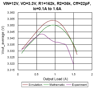
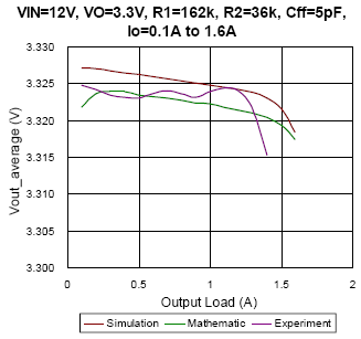
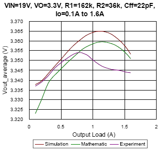
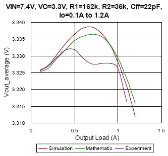
Figure 8. The comparison of simulation, mathematic and experiment results under DEM condition
|
|
(a)
|
(b)
|
|
(c)
|
|
|
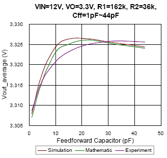
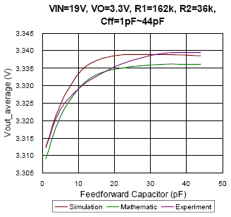
Figure 9. The comparison of simulation, mathematic and experiment results under CCM condition
|
In Figure 8, the average output voltage with regard to different output load under DEM is depicted. From Figure 8(a) to Figure 8(c), the converter setup with the same feed-forward capacitor of 22pF, and with different input voltage changes from 7.4V to 19V separately. The result appears that the mathematic results almost fit the simulation result with deviance smaller than 0.2%. Especially as the duty approaches to 0.5, take Figure 8(a) as an example, due to the output voltage ripple is very similar to sinusoidal waveform, the mathematic result can well estimate the simulation result with deviance smaller than 0.07%. However, the experiment result seems much different with simulation and mathematic results at some conditions. Possible reasons may be the PCB layout, noise disturbance, the regulation of internal LDO and the parasitic components…etc. Nevertheless, the factors that affect the average output voltage in experiment are hard to be implemented in simulation and calculation. In other hands, it can be observed that the feed-forward capacitor will affect the average output voltage. Compare Figure 8(c) with Figure 8(d), the Cff value of prior one is 22pF, the maximum output voltage occurs as load current is 1A instead of no load, and the Cff of latter one is 5pF, the maximum output voltage occurs as no load. It represents that the feed-forward compensator plays an important role in design.
In Figure 9, the relationships of average output voltage and feed-forward capacitor in CCM are presented. As the input voltage changed, the trend of output voltage will also be different. That is, it can’t take one result as the reference for every condition. Unlike the comparison results in DEM, the experiment result is much similar to simulation and mathematic results in CCM for each condition. The maximum deviance between simulation and experiment result is smaller than 0.15%. Moreover, the impact of thermal issue on voltage regulation is not considered in this CCM guess model, one may misunderstand it as the same with the reason of feed-forward compensator.
5. Conclusions
In the application note, the derivation and description of dc offset in both CCM and DEM are well presented. An example has also given to verify the accuracy of mathematic result, the deviance of simulation and mathematic is always smaller than 0.2% whether in CCM or DEM. The well prediction of the mathematic result can reduce the effort and time on simulation setup during design. However, there are still many challenges on the estimation for practical hardware implement. Like the PCB layout, noise disturbance, the regulation of internal LDO and the parasitic components…etc. Many of them are not easy to be forecast and modeled. After all, the additional dc offset which is generated from feed-forward compensator can’t be ignored in practical application, and the optimum design for converter can be completed through accurate mathematic analysis.